We take your privacy very seriously, please agree to all cookies used when you visit our website. More information about the processing of personal data could be found inPrivacy Policy
Second-generation High-performance Isolated Dual-channel Gate Driver


NSI6602V is the second-generation high-reliability isolated dual-channel gate driver IC, which enhances anti-interference capability and drive capability, reduces power consumption, and improves the withstand voltage of the input side. It can drive power transistors with switching frequencies up to 2MHz. Each channel output can provide a maximum source/sink current capability of 6A/8A with a fast 25ns propagation delay and a maximum delay match of 5ns. Minimum common-mode transient immunity (CMTI) of 100kV/us improves system robustness. The maximum supply voltage of the driver is 28V, and the input side accepts supply voltages from 3V to 18V. All supply voltage pins support undervoltage lockout (UVLO). In addition, multiple undervoltage points are available. The minimum undervoltage point supports 4V and can be used to drive GaN power devices. Multiple packages are available. The minimum package is the 4*4mm LGA package, which can be used in applications with high power density requirements. According to UL1577, the NSI6602V provides 2500Vrms isolation with the 5*5mm LGA13 package, 3000Vrms isolation with the SOP16 narrow-body package, and 5700Vrms isolation with SOW16 and SOW14 wide-body packages. With all these outstanding features, NSi6602V is suitable for switching power supply systems which require high reliability, high power density and high efficiency.
Product Features
• Isolated dual-channel driver
• Input side supply voltage: 3V-18V
• Driver side supply voltage: Absolute max rating 30V, with UVLO
• Peak 6A/8A source/sink current capacity
• High CMTI: 150kV/us
• 25ns typical propagation delay
• 5ns maximum delay matching
• 6ns maximum pulse width distortion
• Programmable dead time
• Enabling pins: NSi6602N Disable (high level off), NSi6602N Enable (high level on)
• Acceptable minimum input pulse width 15ns
• Working temperature: -40°C~125°C
• Package form: LGA13 (4*4mm), LGA13 (5*5mm), SOW14, SOW16, SOP16
• AEC-Q100 qualified
Safety Certificate
• UL1577 certification:
LGA13: 2.5kVrms for 1 minute
SOIC14(300mil): 5kVrms for 1 minute
SOIC16(300mil): 5kVrms for 1 minute
SOIC16(150mil): 3kVrms for 1 minute
• CQC certification: GB4943.1 -2011
• CSA certification: components 5A qualified
• VDE certification: DIN V VDE V 0884-11: 2017-1
Application
• Isolated DC-DC and AC-DC power supplies for servers, telecom and industry
• DC-AC solar inverter
• Motor driver and EV charging
• UPS and battery charger
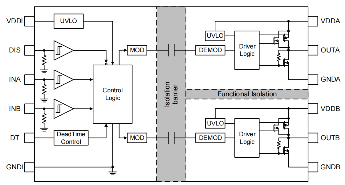
Functional Block Diagram


For more product information, please contact us.
Thank you for your inquiry.
Please provide the following information and we will contact you as soon as possible, thank you.