2022/03/01
Recently, two power management chips (high efficiency and low EMI isolation power chip and fast large conversion ratio DC-DC converter chip) designed by Professor Cheng Lin from the National Demonstration Microelectronics School of University of Science & Technology of China were presented at the highest level conference in the field of integrated circuit design - IEEE International Solid-State Circuits Conference (ISSCC).The first author of this study titled “A 1.2W 51%-Peak-Efficiency Isolated DC-DC Converter with a Cross-Coupled Shoot-Through-Free Class-DOscillator Meeting the CISPR-32 Class-B EMI Standard” published in ISSCC2022 is Pan Dongfang, a special associate professor at the School of Microelectronics, University of Science and Technology of China, Professor Cheng Lin is the corresponding author, and NOVOSENSE is the partner of the Paper.
High-efficiency low-EMI isolation power supply chip
As the size of the isolated power supply becomes smaller and smaller, the frequency and power density of the internal power oscillation signal become higher and higher. Isolated DC-DC converters often become sources of radiation, leading to electromagnetic interference (EMI).The traditional methods to reduce EMI of isolated DC-DC converter are mostly limited to the board level, the development cost is high and the EMI radiation problem cannot be solved thoroughly. In this paper, a symmetric class-D oscillator is proposed to reduce the EMI radiation by reducing the common-mode current of the isolated power supply system at the chip level. Meanwhile, the dead-zone control method can be used to avoid the instantaneous short-circuit current from the power source to the ground. In addition, the proposed architecture only adopts low-voltage power tubes, which effectively improves the conversion efficiency of the oscillator and reduces the chip cost.

Figure 1: Circuit structure and EMI test results of isolated power supply chip
The final test results show that the chip achieves 51% peak conversion efficiency and a maximum output power of 1.2W, which has passed CISPR-32 class-B EMI radiation international standard in a special 10-meter field darkroom. The research result was published in ISSCC2022 titled “A 1.2W 51%-Peak-Efficiency Isolated DC-DC Converter with a Cross-Coupled Shoot-Through-Free Class-DOscillator Meeting the CISPR-32 Class-B EMI Standard”. The first author is Pan Dongfang, a special associate professor at the School of Microelectronics, University of Science and Technology of China, Professor Cheng Lin is the corresponding author, and NOVOSENSE is the partner of the Paper.This is the second consecutive ISSCC paper published by the research group in the field of isolated power chip design.

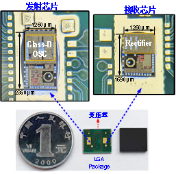
Figure 2: Isolation power supply chip and package photo
Fast large conversion ratio DC-DC converter chip
Single-stage large conversion ratio DC-DC converter has broad application prospects in data centers, 5G communication base stations and other fields because of its advantages of low transmission line loss and high comprehensive efficiency. The existing large conversion ratio DC-DC converters mostly adopt the hybrid topology of multi-phase DC-DC converters combined with series capacitors to extend the equivalent conversion ratio, but the load transient response speed is limited by the multi-phase fixed phase difference and the multi-phase structure cannot be turned on simultaneously.

Figure 3: Fast high conversion ratio DC-DC converter circuit structure and chip photo
Based on the topology structure of two-phase series capacitive DC-DC converter, a voltage mode PWM control method with double feedback loop is proposed to realize the modulation of output voltage and series capacitor voltage. Meanwhile, the fast transient response technology is also proposed, which not only overcomes the shortcoming of the traditional PWM control method that the loop response speed is related to the load jump time, but also improves the response speed of the converter by using two-phase inductive current synchronous charging of the load. The final test results show that the recovery time of this study is only 0.9ms under the load jump of 3A current, which achieves the fastest load transient response speed among similar studies. The study result was published on ISSCC2022 titled “A 12V/24V-to-1V DSD Power Converter with 56mV Droop and 0.9µs 1% Settling Time for a 3A/20ns Load Transient. The first author is Yuan Jingyi, PhD student of the School of Microelectronics, USTC, and Professor Cheng Lin is the corresponding author.

Figure 4: Load transient test results of DC-DC converter chip
The two studies mentioned above were funded by the National Natural Science Foundation of China, the Ministry of Science and Technology and the Chinese Academy of Sciences.
ISSCC is the most advanced chip technology publishing place in the world, which has attracted great attention in the academic and industrial circles, and is also known as the "Chip Olympics". ISSCC2022 was held online from February 20 to 28 this year. ISSCC conference official website: https://www.isscc.org/